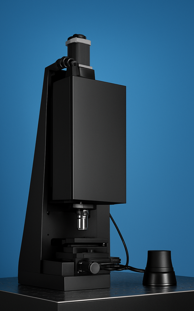
QP12-Nanoprofilometer
Revealing the True Geometry of the Nano-World
Beyond Imaging
Beyond Contact
Beyond Limits
Engineered for applications where accuracy is critical and details matter. Utilizing advanced white-light interferometry, it delivers fast, non-contact three-dimensional surface characterization with nanometer-scale vertical resolution.
Innovative Technologies for Advanced Measurement Applications
At QPhoton, we are redefining the future of precision surface metrology. Combining advanced optical engineering with state-of-the-art interferometric technology, we develop solutions that empower industries to measure, analyze and innovate with confidence.
PRECISION: Enhanced accuracy.
SPEED: Rapid measurements.
NON-CONTACT: Safe for samples.
VERSATILITY: Multi-surface analysis.
RESOLUTION: Fine detail capture.
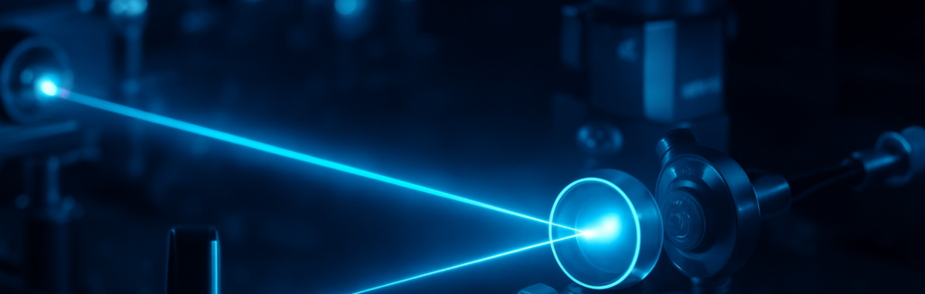
Discover the superiority of white-light interferometry technology.
White-light interferometry offers significant advantages over traditional measurement techniques. By utilizing the full spectrum of light, this method enables precise surface profiling without the need for physical contact, ensuring the integrity of delicate samples. The increased speed of measurements allows for efficient high-throughput analysis, making it an ideal solution for modern semiconductor and MEMS applications. The non-contact nature of the technology not only protects sensitive surfaces but also reduces wear and tear on measuring equipment, leading to longer instrument life.
Advanced Surface Analysis
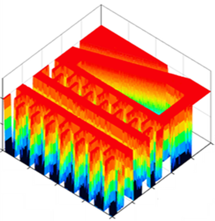
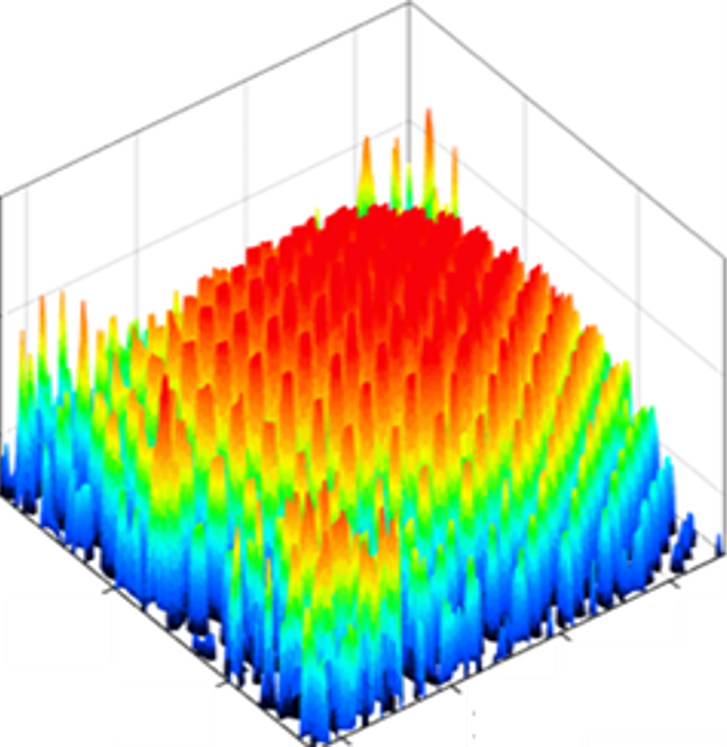
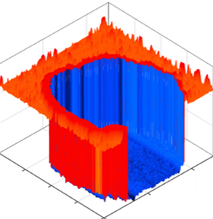
The QP12 excels in advanced surface analysis, delivering unmatched precision for characterizing complex surfaces across a wide range of applications. While highly specialized for semiconductor and MEMS metrology, it is equally capable in thin-film analysis, precision machining and optical component inspection. By generating high-resolution 3D topography maps, the system allows users to visualize and analyze surface characteristics effectively. The software processes comprehensive spatial and profile roughness metrics, capturing step heights with remarkable accuracy and assessing coatings with unparalleled detail.
Competitive Edge Specification
| Specification | Description |
|---|---|
| 3D surface measurement method | WLI |
| Depth measurement accuracy | < 5 nanometers |
| Lateral measurement accuracy | < 500 nanometers |
| Microscope objective lens | Mirau, Linnik 50x, 40x, 20x, 10x |
| Field of view (10x objective) | 1×1 mm² |
| Camera | 5 megapixels, monochrome |
| Light source | LED |
| Light Source Central Wavelength | 620-650 nanometers |
| Z-Axis (Axial) Travel Range | 0-100 micrometers |
| Z-Axis Positioning Precision | 1 nanometer |
| Z-Axis Positional Stability | 1 nanometer |
| Minimum Z-Axis Resolution | 1 nanometer |
| XY-Axis (Lateral) Travel Range | 15 millimeters |
| Control capability | Computer-user (software) |
| Sample holder | Customizable |